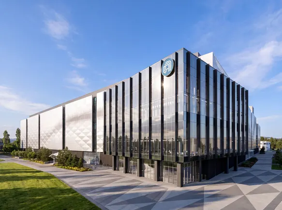
GlobalFoundries has announced a major step forward in semiconductor manufacturing with the construction of two new fabs at its Malta, New York site, as part of a $21 billion U.S.-Japan trade and investment initiative. This development is set to significantly enhance U.S. semiconductor production capacity and bolster critical supply chains, particularly for the automotive and industrial sectors.
What Happened
GlobalFoundries, a leading semiconductor manufacturer headquartered in Malta, New York, will construct two new 300mm semiconductor fabs under a trade agreement between the United States and Japan. Announced on October 14, 2026, this initiative will see Japan investing up to $21 billion into the project, aiming to accelerate U.S. semiconductor manufacturing capabilities. The first phase includes an initial $10 billion investment to build the first fab, with an additional $10 billion allocated for a second fab. Groundbreaking for the first fab is expected later this year, with operations slated to begin in 2029. When fully operational, each facility will produce approximately 900,000 wafers annually, creating over 1,000 skilled jobs in New York's capital region.
This partnership also involves collaboration with Japan-based Renesas Electronics Corp., which views the expanded capacity at GlobalFoundries’ New York site as an extension of its production capabilities. Such cooperation underscores the growing demand for technologies supporting smart vehicles and automated industrial systems.
What This Means for Your Business
The construction of these fabs represents a significant opportunity for businesses involved in the semiconductor supply chain, including those in construction, engineering, and technology sectors. The enhanced production capacity will meet the increasing demand for advanced semiconductors vital to communications infrastructure, data centers, and connected devices. For contractors and suppliers, this project offers substantial procurement and partnership opportunities, potentially leading to long-term contracts and collaborations.
Additionally, the reallocation of $955 million from an existing CHIPS and Science Act award towards investments in silicon photonics and advanced packaging at GlobalFoundries' facilities in New York and Vermont emphasizes the strategic importance of domestic semiconductor capabilities. Companies involved in these areas may find expanded opportunities to contribute to and benefit from these developments.
What US Operators Should Watch
Key dates to monitor include the groundbreaking for the first fab expected later this year and its opening set for 2029. The subsequent phase will involve the construction of a second fab, with timelines for this phase yet to be detailed. Businesses should also track the progress of related investments in silicon photonics and advanced packaging, as these technologies will be critical to future communications infrastructure and data center operations.
Furthermore, the semiconductor industry should remain vigilant regarding compliance with regulations such as the Cybersecurity Maturity Model Certification (CMMC) and updates to the CHIPS Act, which may impact operational and funding aspects. The U.S. Department of Commerce's 4% equity stake in GlobalFoundries also highlights potential shifts in public-private partnerships that could influence future policy and funding directions.
Source: [Supply Chain Dive]. Read the original story ->
Is your firm ready for what’s next?
VisioneerIT helps AECM and government contractors modernize operations, achieve compliance, and implement AI.
Explore VisioneerIT Solutions →